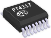
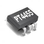
The PT4317 RF chip is a low power single chip OOK/ASK superheterodyne receiver for the 315MHz and 434MHz frequency bands that offers a high level of integration and requires few external components. The PT4317 consists of a low-noise amplifier (LNA), down-conversion mixer, SAW-based local oscillator, on-chip gm-C band-pass filter, intermediate frequency (IF) limiting amplifier stage with received-signal- strength indicator (RSSI), and analog baseband data recovery circuitry (data filter, peak detector, and data slicer). The PT4317 chip is available in a 16-pin SSOP package.
FUNCTION DESCRIPTION
POWER SUPPLY
PT4317 includes an internal voltage regulator to supply power to all receiver blocks. Only the VDD5 pin (pin 9) must be connected to the external supply voltage, along with series-R, shunt-C filtering. Bypass capacitors should be placed as close as possible to the voltage regulator output pin (pin 6). The PT4317 chip supports operation over the supply voltage range from 2.4V to 5.5V.
RF FRONT-END
The RF front-end of the receiver part employs a superheterodyne architecture that achieves good performance characteristics, including low noise figure, high voltage conversion gain, and excellent reverse isolation. The RF front-end down-converts the input radio frequency (RF) signal into an intermediate frequency (IF) signal at 1.8MHz. According to the block diagram, the RF front-end consists of an LNA, down-conversion mixer, and a surface acoustic wave (SAW) oscillator signal with buffer amplifier to drive the mixer’s LO input. The output of the RF chip front-end is fed into the IF chain for channel-select filtering and demodulation.
The RF downconverter does not include inherent suppression of the image frequency. Depending upon the particular application and the system's environmental conditions, a RF front-end filter may be added. If image rejection or good blocking immunity is a relevant system parameter, a band-pass filter must be placed in front of the LNA. This filter may be a SAW or LC-based filter (e.g. helix type).
The chip input pin (pin 3) may be matched to 50Ω with a shunt inductor from the RF input pin to ground and a series capacitor from the RF input to the antenna. An example of the input matching network is shown in the figure below and the input impedance of the PT4317 for 315 and 434MHz frequency bands is listed in the right-hand side table. The component values given in the BOM for the application circuit shown on page 2 are nominal values only. Actual inductor and capacitor values may be different, depending upon the PCB material, PCB thickness, ground configuration, and length of PCB traces.
IF CHANNEL SELECT FILTER (CSF)
Out-of-band interference is rejected by means of a 6th-order Chebyshev gm-C filter centered at a frequency of 1.8MHz. To compensate for manufacturing tolerances, the IF CSF is auto-tuned after power-up. The IF filter auto-tuning mechanism requires an external resistor (R2) of 270K. By the way, the variation of the value of R2 within 1% is better.
SAW OSCILLATOR
The SAW oscillator of RF chip is configured as a Pierce oscillator, but consists of a cascade of three amplifiers instead of a single amplifier. Although the circuit configuration is quite similar to the conventional Pierce oscillator, this configuration is capable of generating a much higher value of negative resistance. The SAW resonator is connected between pin 15 (OSCIN) and pin 16 (OSCOUT).
The capacitors (C8 and C9) connected from pin 15 (OSCIN) and pin 16 (OSCOUT) to ground is used for adjusting the oscillation frequency. In general, those capacitors are unnecessary if the frequency drift can be ignored. The SAW oscillator circuit is shown in the left-hand side figure below, and an equivalent circuit of a SAW resonator is shown on the right-hand side. The component values of the equivalent circuit are also listed below for reference.
For down-converting the RF signal to the IF frequency, a suitable SAW oscillation frequency must be chosen. In the PT4317 RF chip, since the center frequency of the IF CSF is located at 1.8MHz, the following equation may be used to calculate an appropriate SAW oscillator frequency: SAW Oscillator Freq. = TX Freq. ± 1.8 MHz
In addition to a SAW resonator, the resonant circuit may also be achieved by an L-C tank circuit. A recommended circuit for an L-C tank is shown in the following figure.
LIMITER/RSSI
The limiter is an AC coupled, multi-stage amplifier with a cumulative gain of approximately 70dB that has a band-pass characteristic centered near 1.8MHz. The –3dB bandwidth of the limiter is around 2MHz. The limiter circuit also produces an RSSI voltage that is directly proportional to the input signal level with a slope of approximately 10mV/dB. This signal is used by the succeeding baseband circuitry to demodulate ASK-modulated receive signals.
DATA FILTER
The RF chip data filter is also implemented as a 2nd-order low-pass Sallen-Key filter. The pole locations are set by the combination of two on-chip resistors and two external capacitors. Adjusting the value of the external capacitors changes the corner frequency and allows for optimization with different data rates. The corner frequency should be set to approximately 1.5 times the highest expected data rate from the transmitter. An ideal Sallen-Key filter is shown below.
Utilizing the on-board voltage follower and the two 100K on-chip resistors, a 2nd-order Sallen-Key low pass data filter may be constructed by adding two external capacitors between pins 7 (DFFB) and 8 (DSP) and to pin 10 (OPP) as depicted in the Application Circuit (see page 2). The following table shows the recommended values of the capacitors for different data rates.
PEAK DETECTOR
The peak detector generates a DC voltage which is proportional to the peak value of the received data signal. An external R-C network is necessary. The peak detector input is connected to the data filter output, which is connected to pin 8 (DSP), and its output signal can be used as a reference for the data slicer. The R-C time constant is calculated with the driving current of the data filter, 250μA. The following table shows the recommended values of the resistor and capacitors for different data rates.
DATA SLICER
The data slicer consists chiefly of a fast comparator, which allows for a maximum received data rate up to 50Kb/s. The maximum achievable data rate also depends upon the IF filter bandwidth. Both data slicer inputs are accessible off-chip to allow for easy adjustment of the slicing threshold. The output delivers a digital data signal (CMOS level) for subsequent circuits. The self-adjusting threshold on pin 12 (DSN) is generated by an R-C network or peak detector depending upon the baseband coding scheme.
The suggested data slicer configuration uses an internal 25KΩ resistor connected between DSN and DSP with a capacitor from DSN to ground as shown in the following figure. The cut-off frequency of the R-C integrator must be set lower than the lowest frequency appearing in the data signal to minimize distortion in the output signal.
DEMODULATION
Using different circuit combinations, the PT4317 RF chip is capable of achieving three demodulation modes: “Peak Mode”, “Squelch Mode” and “Average Mode.”
PEAK MODE
The peak detector circuit can contributes an instantaneous voltage jump on node “DSN” through capacitive voltage divider formed by C7 and C12. After the jump, the voltage on node “DSN” will decay to a steady–state value determined by the resistive divider formed by Rin and R5. By selecting the suitable value of R5, C7 and C12, the threshold voltage for comparison can be rapidly set through the help of peak detector circuit (see the ”PEAK DETECTOR” section).
SQUELCH MODE
In the absence of a RF chip signal, the data filter outputs a DC voltage with a time-varying noise which the peak-to–peak voltage value is around 20mV. The noise makes the non-inverting input voltage of the data slicer swing back and forth across the DSN threshold voltage, causing the comparator’s output to switch back and forth between the supply voltage and ground randomly. The squelch mode operation adds a threshold deviation (DC offset) on the DSN threshold that stop the effect. However, the sensitivity will be sacrificed. The recommended value for the resistor R6 is 1.2MΩ(The sensitivity loss is about 4dB). The DC offset can be adjusted by changing the resistance of R6 and VREG voltage. A larger DC offset will introduce more sensitivity loss.
AVERAGE MODE
When the “Average Mode” has been set according to the figure shown in the DATA SLICER section above, the DATA output will exhibit a toggling behavior similar to random noise. In this mode, better sensitivity may be achieved, but noise immunity is worse than in “Peak Mode.”
SENSITIVITY AND SELECTIVITY
In digital radio systems, sensitivity is often defined as the lowest signal level at the receiver input that will achieve a specified bit error rate (BER) at the output. The sensitivity of the PT4317 receiver is typically –106dBm (ASK modulated with 2Kb/s, 50% duty cycle square wave) to achieve a 0.1% BER when its input is matched for a 50Ω signal source.
The selectivity is governed by the response of the receiver front-end circuitry, the IF channel select filter (CSF), and the data filter. Note that the IF filter provides not only channel selectivity, but also the interference rejection. Within the pass band of the receiver, no rejection for interfering signals is provided.
POWER-DOWN CONTROL
The RF chip enable (CE) pin controls the power on/off behavior of the PT4317. Connecting CE to “HIGH” sets the PT4317 to the normal operation mode; connecting CE to “LOW” sets the PT4317 to standby mode. The current consumption of the PT4317 is lower than 1μA in standby mode. Once enabled, the PT4317 requires
ANTENNA DESIGN
For a λ/4 dipole antenna and operating frequency, f (in MHz), the required antenna length, L (in cm), may be calculated by using the formula L=7132/f
For example, if the frequency is 315MHz, then the length of a λ/4 antenna is 22.6 cm. If the calculated antenna length is too long for the application, then it may be reduced to λ/8, λ/16, etc. without degrading the input return loss. However, the RF input matching circuit may need to be re-optimized. Note that in general, the shorter the antenna, the worse the receiver sensitivity and the shorter the detection distance. Usually, when designing a λ/4 dipole antenna, it is better to use a single conductive wire (diameter about 0.8mm to 1.6mm) rather than a multiple core wire.
If the antenna is printed on the PCB, ensure there is neither any component nor ground plane underneath the antenna on the backside of PCB. For an FR4 PCB (εr=4.7) and a strip-width of 30mil, the length of the antenna, L (in cm)
PCB LAYOUT CONSIDERATION
Proper PCB layout is extremely critical in achieving good RF chip performance. At the very least, using a two-layer PCB is strongly recommended, so that one layer may incorporate a continuous ground plane. A large number of via holes should connect the ground plane areas between the top and bottom layers. Note that if the PCB design incorporates a printed loop antenna, there should be no ground plane beneath the antenna.
Careful consideration must also be paid to the supply power and ground at the board level. The larger ground area plane should be placed as close as possible to the VSS and VSSLNA pins. To reduce supply bus noise coupling, the power supply trace should be incorporate series-R, shunt-C filtering as shown below.
If the power source is capable of supplying a stable voltage, C’ may be ignored. In some applications, the DC source may be supplied from a simple AC-DC transformer. In such cases, the DC voltage level could be unstable and may adversely affect ASK/OOK receiver sensitivity. A solution may be to increase C to an appropriately large value while continuing to make the power source as stable as possible.
Finally, in an RF system, it is extremely important to keep the LNA or RF signal traces away from large voltage swing signals and digital data signal traces to avoid unnecessary interference. A representative layout of a PT4317 demo-board is shown on page 14.
IMPORTANT NOTICE
Princeton Technology Corporation (PTC) reserves the right to make corrections, modifications, enhancements, improvements, and other changes to its products and to discontinue any product without notice at any time.
PTC cannot assume responsibility for use of any circuitry other than circuitry entirely embodied in a PTC product. No circuit patent licenses are implied.
| Part | Value - 315MHz | Value - 433.92MHz | Unit | Description |
|---|---|---|---|---|
| L1 | 47n | 27n | H | Antenna input matching, coil inductor. |
| C1 | 1.8p | 1.8p | F | Antenna input matching. |
| C2/C4 | 100n | 100n | F | Power supply de-coupling capacitor. |
| C3 | 470p | 470p | F | Data filter capacitor. |
| C5 | 150p | 150p | F | Data filter capacitor. |
| C6 | 100n | 100n | F | Peak detector bypass capacitor(average mode) |
| C7 | 22n | 22n | F | Data slicer threshold charge capacitor. |
| C8/C9 | - | - | F | SAW oscillator frequency trimming capacitors. — — F SAW oscillator frequency trimming capacitors. |
| R1/R4 | 10K | 10K | Ω | MCU interface resistor (option). |
| R2 | 270K | 270K | Ω | IF filter tuning resistor |
| R3 | 10 | 10 | Ω | Power supply de-coupling resistor (option). |
| S1 | 316.8 | 435.72 | MHz | SAW oscillator. |
| U1 | PT4317 IC | PT4317 IC | U1 | Receiver chip. |
Specifications
- Low current consumption (4.7mA at VDD=5.0V)
- 2.4V to 5.5V supply voltage operation range
- Optimized for 315MHz or 434MHz ISM Band
- Saw-based oscillator with low frequency drift
- On-chip IF filter with better adjacent channel rejection capability
- Power down mode with very low supply current (< 1µA)
- Low external parts count
- 16-pin SSOP package
- Applications:
- Remote Keyless Entry (RKE) systems
- Remote control systems
- Garage door openers
- Alarm systems
- Security systems
- Wireless sensors
- Order Information
- Valid Part Number: PT4317-X
- Package Type: 16 Pins, SSOP, 150mil
- Top Code: PT4317-X
Main Products
RF Chip, Radio Frequency ID Chip, Transmitter IC
Related Products
Contact Detail
-
Sales ContactLarry Lee
-
Address2F, No. 233-1, Baociao Road, Sindian Taipei 23145 Taiwan
-
Tel886-2-66296288
-
Fax886-2-29174598
-
E-mail
-
URL


